Quantum computing systems require far more than stationary processing qubits. To scale into distributed networks and multi-processor clusters, quantum processors need deterministic control interfaces, high-fidelity readout mechanisms, and seamless bridges to optical photons that can transmit quantum states between physical nodes.
On 15 October 2026, Optica reported a significant milestone in hybrid quantum photonics: a monolithic platform that dramatically strengthens the interaction between traveling light and quantum memory states stored in diamond. Published in Optica Quantum, the experimental architecture combines high-index gallium phosphide (GaP) nanophotonic cavities with diamond substrates hosting silicon-vacancy (SiV) color centers. The demonstration marks an essential engineering step toward modular, optically linked quantum processing nodes.
Read the official research announcement from Optica.
The Interface Problem: Coupling Solid-State Qubits with Photons
Many leading solid-state quantum platforms store quantum information in physical spin states that remain stationary within a chip substrate. While these stationary qubits excel at localized gate execution and quantum memory storage, they cannot easily travel over physical distances.
Photons (the fundamental particles of light) provide the optimal medium for transferring quantum information across optical fibers and free-space channels. However, creating a high-fidelity interface between stationary matter qubits and traveling optical photons has historically posed severe engineering bottlenecks:
- Weak Light-Matter Coupling: In bulk materials, photons interact very weakly with individual atomic-scale quantum emitters, resulting in low photon collection efficiency and high loss.
- Spectral Inhomogeneity and Decoherence: Surrounding material strains and charge fluctuations frequently shift emission wavelengths, degrading indistinguishability.
- Integration Challenges: Traditional optical components are bulky and difficult to align deterministically with microscopic quantum defects.
Overcoming these limitations demands specialized hybrid photonic integrated circuits (PICs) that can tightly confine optical fields precisely at the location of quantum emitters.
The GaP-on-Diamond Architecture: 600 Nanophotonic Cavities at 99.5% Yield
To maximize coupling without degrading emitter coherence, the research team engineered a complementary dual-material platform:
- Synthetic Diamond Substrate: Hosts negatively charged silicon-vacancy (SiV) centers. SiV centers possess inversion symmetry, making them naturally insensitive to first-order electrical noise and capable of emitting coherent, narrow-linewidth photons.
- Gallium Phosphide (GaP) Waveguides & Cavities: GaP exhibits a high refractive index ($n \approx 3.3$), broad optical transparency across the visible and near-infrared spectrum, and negligible autofluorescence at SiV emission wavelengths ($\sim 737\text{ nm}$).
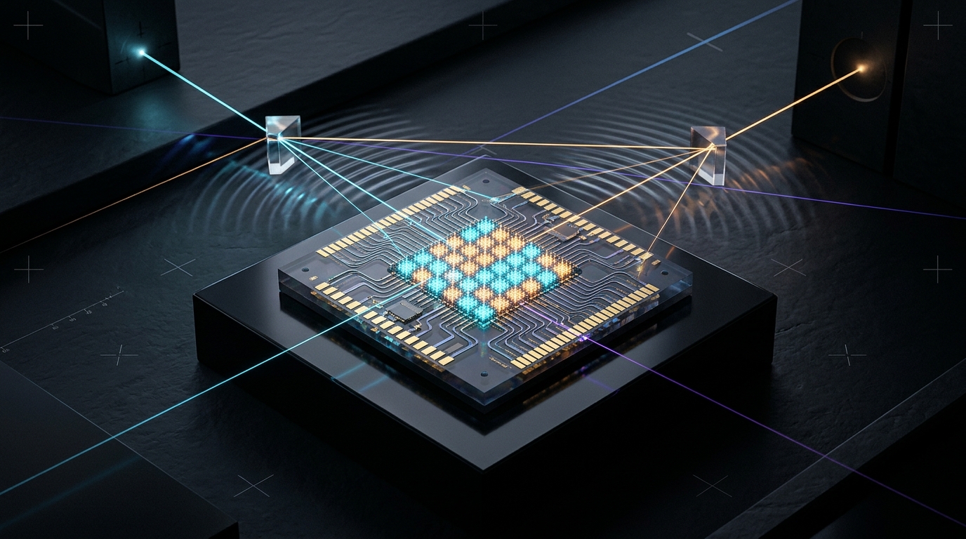
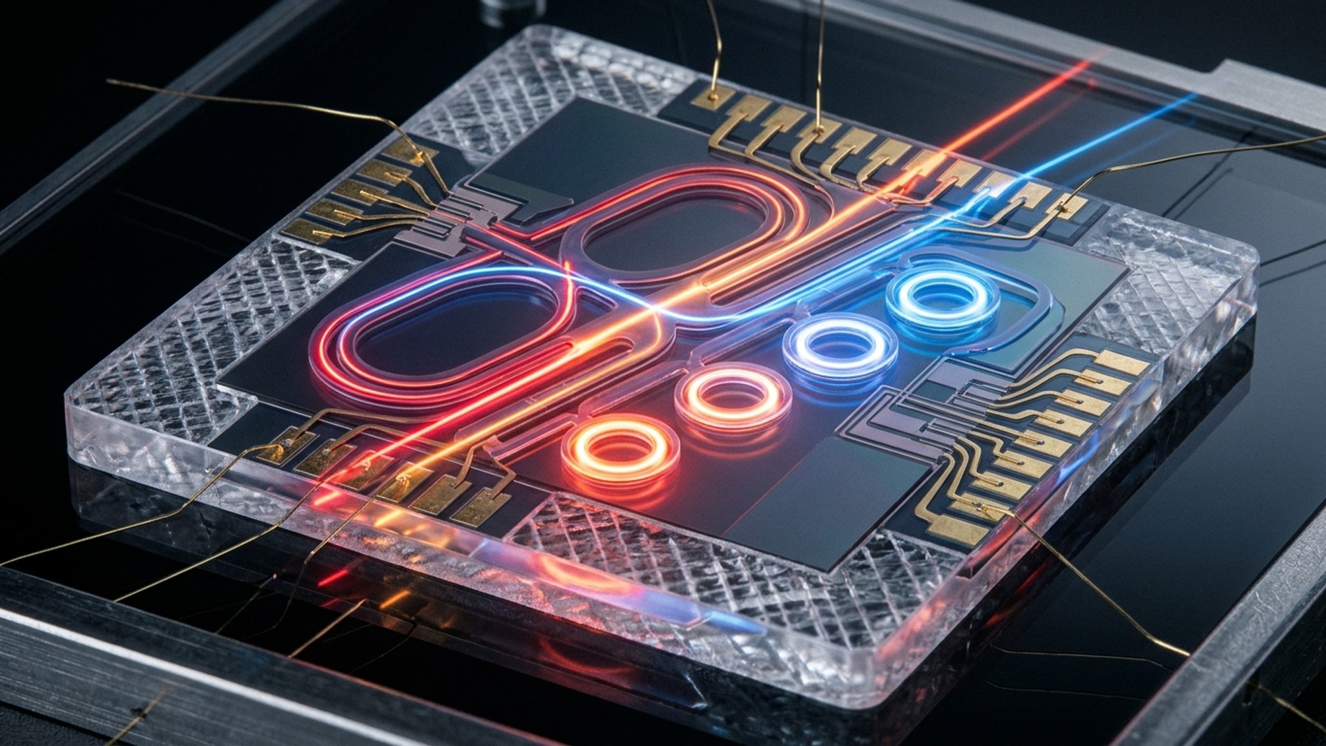
Using a precise nanoscale stamp-transfer manufacturing technique, the team transferred over 600 GaP nanophotonic optical cavities directly onto a single diamond substrate, achieving an unprecedented fabrication yield of 99.5%. This high yield is a vital milestone for moving quantum photonics from bespoke single-device physics experiments toward wafer-scale photonic integration.
Enhanced Light-Matter Coupling and Single-Shot Spin Readout
By confining optical modes to sub-wavelength volumes, the GaP nanocavities enhance the spontaneous emission rate into guided modes via the Purcell effect.
The researchers demonstrated:
- Strong Optical Coupling: Light-matter interaction was sufficiently robust to resolve the specific electron spin states of individual SiV centers through resonant scattered transmission.
- Single-Shot Spin Readout: The platform demonstrated single-shot readout of the electron spin state under cryogenic operating conditions, eliminating the need for prolonged averaging that can introduce decoherence.
- Deterministic Waveguide Routing: Photons emitted by the diamond centers coupled directly into integrated GaP waveguides for on-chip routing.
This development provides an on-chip physical interconnect that links solid-state spin memories directly to guided optical channels.
Implications for Distributed Quantum Networking
Scalable quantum computing will likely mirror classical high-performance computing, evolving from isolated mainframes to modular clusters linked by high-bandwidth optical interconnects. A functional quantum network requires:
- Local processing nodes to perform multi-qubit gates.
- Photonic quantum repeaters to overcome exponential transmission attenuation.
- High-efficiency spin-photon interfaces that convert stationary qubit states into polarization or time-bin optical qubits.
The GaP-on-diamond platform directly tackles the interface challenge. By integrating hundreds of high-quality factor cavities on a single substrate, it provides a scalable blueprint for on-chip multiplexing, where multiple quantum repeaters or network channels can be integrated into a compact microchip footprint rather than sprawling across optical tables.
Operating Regimes: Cryogenic Diamond Nodes vs. Ambient Photonic Interconnects
It is essential to distinguish the operating conditions of solid-state emitter chips from the room-temperature optical channels that connect them:
- The GaP-on-Diamond Experiment: The SiV centers in this work operated within a liquid-helium cryostat at approximately $4\text{ K}$. Deep cryogenic temperatures remain necessary for solid-state color centers to suppress acoustic phonon scattering that would otherwise cause rapid dephasing of the spin states.
- The Optical Interconnect Layer: The photons generated and routed through the GaP waveguides and subsequent fiber networks propagate seamlessly at room temperature through ordinary telecom infrastructure.
While diamond-based matter nodes require refrigeration, the optical links that interconnect them are ambient. Understanding these physical boundaries helps contextualize how diverse photonic technologies integrate across the broader quantum ecosystem.
Context in the Evolving Quantum Photonics Landscape
The GaP-on-diamond milestone highlights a clear convergence across modern quantum engineering: hardware development is expanding from standalone qubit fabrication to the optical networks required to link them.
At OJANVU Quantum Labs, our core focus is advancing room-temperature photonic quantum computing using continuous-variable (CV) optics and squeezed states of light. While the GaP-on-diamond demonstration utilizes discrete-variable (DV) single-photon emitters in diamond, both approaches rely on the same fundamental advantage: photons provide the ultimate carrier for high-speed, low-loss, room-temperature quantum information. Progress in nanophotonic cavity fabrication, waveguide routing, and optical coupling benefits the entire photonics discipline.
Key Milestones for Future Integrated Quantum Platforms
While fabricating 600 cavities with 99.5% yield is a landmark achievement, several key engineering hurdles remain before such platforms enable full-scale quantum networks:
- On-Chip Device-to-Device Entanglement: Demonstrating high-fidelity quantum entanglement between multiple distant color centers mediated entirely by on-chip waveguides.
- Integrated Phase Shifters and Active Switching: Incorporating electro-optic modulators to dynamically route photons between network channels without introducing thermal dissipation.
- Fiber Packaging and Insertion Loss: Developing ultra-low-loss fiber-to-chip packaging solutions that preserve optical coherence across long-distance distribution.
- Spectral Tuning: Implementing local strain or Stark-shift tuning to bring distinct emitters into exact spectral resonance across fabrication variations.
Conclusion: Bridging Stationary Qubits and Flying Photons
The realization of practical quantum computation and distributed networking depends on solving interconnect bottlenecks. Hybrid platforms that seamlessly unify high-performance nanophotonics with robust quantum memory systems are turning theoretical networking schemes into manufacturable hardware.
The GaP-on-diamond architecture demonstrated in Optica Quantum is a prime example of this convergence. By turning microfabricated diamond into an efficient photonic transceiver, it brings modular, connected quantum hardware one step closer to reality.
At OJANVU Quantum Labs, we will continue tracking and analyzing foundational breakthroughs in photonics, optical control, and quantum hardware engineering as the industry transitions from proof-of-concept experiments to scalable computational architectures.